In this learning module you'll build a system that uses an ADC chip to measure the voltage over a potentiometer. The ADC chip you'll use is the ADC0831. The quantized voltage will be transmitted to the MicroStamp11 over an SPI serial link. Your system will then transmit this quantized voltage over a wireless IR link and your MicroStamp11 will decode the received frame of data. The value transmitted and received by your MicroStamp11 will be displayed on a serial LCD display (BPI-216). Note that the ADC and LCD subsystems were already built in the earlier learning module covering serial communication.
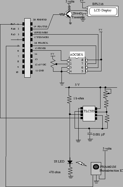
Figure 54 shows the hardware schematic diagram for your system. This schematic was obtained by composing the individual schematic diagrams we showed earlier for the ADC, LCD, and wireless IR link subsystems.
The software side of this project is shown in the following listing.
 #include "kernel.c"
 void main(void){
   int i;
   init();

   OutChar(254);OutChar(1);

   while(1){
     sdata = shiftin(SPI_62kHz);
     sdata &= ~0x80;

     OutChar(254);OutChar(2);
     OutString("S=");OutUDec(sdata);
     OutChar(SP);OutChar(SP);OutChar(SP);
     for(i=0; i<8; i++){
       if((sdata & bit(i))==0){
         OutChar('0');
       }else{
         OutChar('1');
     }}
     OutChar(SP);OutChar(SP);OutChar(SP);

     if(_sbit == 0){
       set_pin(1);
       asm(" sei");
       TMSK1 |= OC4;
       TOC4=TCNT + _bit_time;
       TFLG1 |= OC4;
       asm(" cli");
     }

     OutChar(254); OutChar(192);
     OutString("R=");OutUDec(rdata);
     OutChar(SP);OutChar(SP);OutChar(SP);
     for(i=0;i<8;i++){
       if((rdata & bit(i))==0){
         OutChar('0');
       }else{
         OutChar('1');
       }}
     OutChar(SP);OutChar(SP);OutChar(SP);
   }
 }
 #include"vector.c"
The preceding program consists of a while loop that
has four parts. The fist part using the shiftin
instruction shifts in the converted voltage from the ADC
chip into the variable sdata. The variable
sdata contains the byte that is to be transmitted
over our wireless link. The next part of the main program
displays the transmitted data in sdata on the LCD
display. The LCD display shows both the decimal and binary
versions of sdata. The third part of the program
arms the OC4 interrupt. In this program we'll use
the OC4 interrupt to automatically configure and
transmit the serial frame containing sdata. The
actual code controlling the transmission of data will be
found in the OC4 interrupt handler. The final part
of the program displays the received data on the LCD
display. The received data is held in the global variable
rdata. Our program displays both the binary and
decimal versions of rdata. Note that the main
program doesn't contain the code that actually decodes the
received serial frame. The code that fills the variable
rdata will be found in the interrupt handlers for
the IC1 and OC3 event. In this program, we
coordinate the interaction of these two hardware events in
order to extract rdata from a received frame of
data.
The majority of the work in this learning module is
performed by the interrupt handlers. So we now turn to the
interrupt handlers found in kernel.c. We first look
at the OC4 interrupt handler. Recall that we arm
this handler immediately after a converted voltage has been
shifted into the MicroStamp11. The code segment for the
handler is shown below:
 unsigned int _sbit;
 unsigned int sdata;
 unsigned int _bit_time, _bit_time_2;

 #pragma interrupt_handler OC4han()
 void OC4han(void){
   if(_sbit==0){
    TOC4 = TOC4 + _bit_time_2;
    PORTA &= ~bit(7);
   }
   if(_sbit==1){
    TOC4=TOC4 + _bit_time_2;
    PORTA |= bit(7);
   }
   if((_sbit > 1) & (_sbit<10)){
     TOC4=TOC4+_bit_time;
     if( (sdata & bit(_sbit-2))==0){
       PORTA |= bit(7);
     }else{
       PORTA &= ~bit(7);
     }
   }
   if(_sbit==10){
     TOC4 = TOC4 + _bit_time;
     PORTA &= ~bit(7);
   }
   if(_sbit==11){
     _sbit=0;
     TMSK1 &= ~OC4;
     PORTA &= ~bit(7);
   }else{
     _sbit=_sbit+1;
     TFLG1 |= OC4;
   }
 }

 extern void OC4han();
 #pragma abs_address:0xffe2;
  void (* OC4_handler[])()= { OC4han };
  #pragma end_abs_address
The OC4 interrupt handler uses the global variable
_sbit to control its operation. This variable is
used to record which part of the frame is currently being
transmitted. If _sbit equals zero, then we know that
we are starting the frame. So we set the output high for a
period of ![]() seconds. The actual duration
seconds. The actual duration ![]() is set in
the variable
is set in
the variable _bit_time. The duration ![]() is
stored in the variable
is
stored in the variable _bit_time_2. This first part
transmits the start-bit. After the start bit is
transmitted, we set the line low for ![]() seconds. This
completes the transmission of the start bit. The handler
then begins sending out the information bits. After the
last information bit is sent, our handler transmits a stop
bit of duration
seconds. This
completes the transmission of the start bit. The handler
then begins sending out the information bits. After the
last information bit is sent, our handler transmits a stop
bit of duration ![]() seconds. When the stop bit
transmission is complete, then the OC4 handler disarms
itself. It won't be re-armed until the next AD conversion
takes place.
seconds. When the stop bit
transmission is complete, then the OC4 handler disarms
itself. It won't be re-armed until the next AD conversion
takes place.
The OC4han ISR automatically transmits the converted
byte in sdata over the wireless link. The reception
and decoding of this frame of data is done by the
coordinated use of an input capture and output compare
interrupt. The input capture interrupt is used to detect
the start-bit. Once the start bit has been detected, then
the IC interrupt handler arms the OC3 interrupt event. The
OC3 interrupt is used to read off 8 information bits that
are assumed to be separated by ![]() seconds. The source
code for the IC1 interrupt handler is shown below.
seconds. The source
code for the IC1 interrupt handler is shown below.
 unsigned int _rbit;
 unsigned int rdata, rdata_buf;
 unsigned int _start_frame;
 unsigned int _start_time;
 unsigned int _start_bit_width;

 #pragma interrupt_handler IC1han()
 void  IC1han(void){
   asm(" sei");
   if(TCTL2 == 0x10){
     TCTL2 = 0x20;
     _start_frame = TIC1;
     TFLG1 |= IC1;
   }else{
     if(_start_frame < TIC1){
       _start_bit_width = TIC1 - _start_frame;
     }else{
       _start_bit_width = 65536 - _start_frame + TIC1;
     }
     if(_start_bit_width < (_bit_time_2 + 1000)){
       TOC3 = _start_frame + _start_time;
       rdata_buf = 0xFF;
       TMSK1 &= ~IC1;
       TMSK1 |= OC3;
       TFLG1 |= OC3;
     }else{
       TCTL2 = 0x10;
       TFLG1 |= IC1;
     }
   }
   asm(" cli");
 }

  extern void IC1han();
  #pragma abs_address:0xFFEE;
  void (* IC1_handler[])()={ IC1han };
  #pragma end_abs_address
The IC1 handler is first called on the rising edge of a
received pulse on pin PA2. At this time, we store the
current time in _start_frame and set the next
interrupt to occur on the falling edge. So the next time
the IC1 ISR is called, we know that it was triggered by the
falling edge of the pulse. We then compute the width of
this pulse and store it in _start_bit_width. If the
size of _start_bit_width is consistent with a start
bit of duration ![]() seconds, then we disarm the IC1
interrupt and enable the OC3 interrupt. For the OC3
interrupt, we set its control register
seconds, then we disarm the IC1
interrupt and enable the OC3 interrupt. For the OC3
interrupt, we set its control register TOC3 so it
triggers ![]() seconds after the rising edge of the start
bit. If the received pulse width is not consistent with
the width of a start bit, we then reset the IC1 interrupt
so it begins looking for a rising edge again.
seconds after the rising edge of the start
bit. If the received pulse width is not consistent with
the width of a start bit, we then reset the IC1 interrupt
so it begins looking for a rising edge again.
The IC1 interrupt is used to detect the start bit. After
the start bit is detected, the function IC1han
starts an output compare timer (OC3). The output compare
interrupt OC3 is used to read off the information bits in
the received frame. The source code for the OC3 interrupt
handler is shown below.
 #pragma interrupt_handler OC3han()
 void OC3han(void){

   if(_rbit < 8){
     if((PORTA & bit(2))==0){
       rdata_buf &= ~bit(_rbit);
     }else{
       rdata_buf |= bit(_rbit);
     }
     _rbit = _rbit+1;
     TOC3 = TOC3 + _bit_time;
     TFLG1 |= OC3;
   }else{
    _rbit=0;
    TMSK1 &= ~OC3;
    TMSK1 |= IC1;
    TFLG1 |= IC1;
    TCTL2 = 0x10;
    rdata= rdata_buf;
   }
 }

 extern void OC3han();
 #pragma abs_address:0xFFE4;
 void (* OC3_handler[])()={ OC3han };
 #pragma end_abs_address
The OC3 interrupt handler simply reads the input pin PA2 and
sets the appropriate bit in rdata. (Actually we
construct rdata in a temporary buffer
rdata_buf. When the frame is completely decoded,
then we move rdata_buf into rdata.)
The handler then resets the control register TOC3
so that the next information bit is read ![]() seconds
later. After the OC3 interrupt has been called 8 times,
then we know that all of the information bits have been
read. At this point, we can then reset
seconds
later. After the OC3 interrupt has been called 8 times,
then we know that all of the information bits have been
read. At this point, we can then reset _rbit,
disarm the OC3 interrupt and re-arm the IC1 interrupt so
we are ready to receive the next start bit.