The Motorola 68HC11's SPI interface uses four pins on the
MicroStamp11. These are pins 15-18. They correspond to
bits PD2 and PD5 on PORTD. The clock line comes out
of pin PD4 with the logical name SCK. This line is
a 50 percent duty cycle clock whose rate can be controlled
by the programmer. There are two data lines. The
master-out slave-in (MOSI/PD3) is used to transmit data to
the slave device. The master-in slave-out (MISO/PD2) is
used to receive data from a slave device. In addition to
the clock and data lines, the Motorola 68HC11 has an
additional control line with the logical name SS on
pin PD5. The so-called slave select pin (PD5/SS) is
an optional logical control line that can be used when the
channel is active. It is often used to signal the end or
beginning of a transmission.
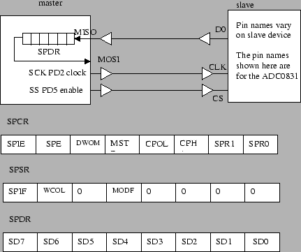
The top drawing in figure 28 shows how
the SPI interface is arranged. The data (MOSI/MISO) pins
are connected to an 8-bit data register SPDR. When
a data transfer operation is performed, this 8 bit register
is serially shifted eight positions and the data is
transmitted or received from the slave. The SPI interface
is controlled by three registers shown in the bottom half
of figure 28. These registers are the
control register SPCR, the status register
SPSR and the data register SPDR. The figure
also shows the logical names for specific bits in these
registers.
As before, rather than discussing the detailed use of the
SPI control registers, we'll introduce two kernel functions
that use the SPI interface. These functions are
shiftout() and shiftin(). The function
shiftout shifts out an 8 bit frame at a specified
rate over the MOSI line. The function shiftin shifts
in an 8 bit frame at a specified rate over the MISO line.
A listing for the shiftout function is given below.
This function takes two arguments, the data (a
single byte) to be transmitted and the rate at which
the communication is to take place. Upon completion the
function returns nothing (void). But shiftout is a
blocking function. This means that the function will
not return until the data has actually been transmitted by
the MicroStamp11.
void shiftout(unsigned char data,unsigned char rate){
    unsigned char dummy;
    DDRD |= 0x38;
    PORTD = 0x00;
    SPCR = 0x50;
    SPCR |= rate;
    SPDR = data;
    while((SPSR & SPIF)==0){};
    dummy=SPDR;
    PORTD |= 0x20;
    PORTD &= ~0x20;
    SPCR = 0x00;
 }
The first line in this function sets the direction state
of the PORTD pins to output. It then zeros PORTD. The
instruction SPCR=0x50 enables the SPI system and puts
the micro-controller in master mode. The rate is then set
and the data is loaded in SPDR. The function then
waits until bit SPIF in the status register
SPSR is set, indicating that the transfer is
complete. The last two lines of code toggle the SS
pin (to signal that the transmission is complete) and the SPI interface is then disabled.
A listing for the shiftin function is also given
below. This function takes a single argument, the
rate at which the data is to be clocked into the
MicroStamp11. Upon completion the function returns the
data to the main routine. Once called, the
function does not return until the data has been received.
So shiftin is also a blocking function call.
 unsigned char shiftin(unsigned char rate){
   unsigned char data;
   DDRD |= 0x38;
   PORTD |= 0x00;
   SPCR=0x50;
   PORTD &= ~0x20;

   SPDR=0; //start SPI
   while((SPSR & SPIF));
   data = SPDR;

   SPCR=0x00;
   return data;
}
The function shiftin() works as follows.
We start by setting the SS line low to signal the
slave to start its operation. In the case of the ADC we'll use in the next section,
this signal initiates the conversion by the ADC0831 chip. We then start the SPI by
loading the register with zero. The function then sits in a while loop until
the SPIF bit in the status register SPSR has been set. Setting this bit
indicates that the SPI's data register is full. In other words, the data transfer
is complete. The contents of the data register SPDR are then
transferred to a local variable (data) which is returned by the
function.