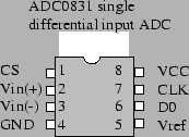
This subsection shows how to use the SPI interface in controlling an 8-bit analog-to-digital converter (ADC). The ADC we'll use is the ADC0831. It is an 8 pin DIP (dual in line package) whose pin out is shown in figure 29. The ADC0831 is an 8-bit successive approximation analog to digital (A/D) converter with a serial I/O port.
The ADC0831 is a differential ADC. This means that
it converts the voltage difference between the positive
and negative input terminals ![]() and
and ![]() on
pins 2 and 3, respectively. This voltage difference is
denoted as
on
pins 2 and 3, respectively. This voltage difference is
denoted as
![]() . When the control
line
. When the control
line CS (pin 1) is set low, then the chip begins
converting ![]() into an 8 bit integer. The LSB of
this integer equals 1/256 of the voltage between the
reference voltage on
into an 8 bit integer. The LSB of
this integer equals 1/256 of the voltage between the
reference voltage on ![]() (pin 5) and ground (pin 4).
We usually tie
(pin 5) and ground (pin 4).
We usually tie ![]() to
to ![]() (pin 8) in order
to get the full conversion range. As noted above, the
conversion is started when the control pin
(pin 8) in order
to get the full conversion range. As noted above, the
conversion is started when the control pin CS (pin
1) is set low. The converted 8 bit integer is then loaded
into a buffer that is clock out over the D0 line
(pin 6) in synchrony to the clock pulses received on the
CLK line (pin 7).
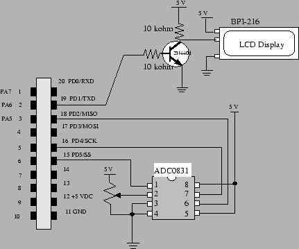
The ADC0831 and the
MicroStamp11's SPI port are connected as shown in figure
30. In this case, we connect
the ADC0831 pin CS to the MicroStamp11's SS
terminal. The MicroStamp11's SRCLK pin is
connected to the ADC0831's CLK pin. Since we are
reading data from the slave device, the ADC's D0
pin is connected to the MicroStamp11's MISO pin.
The voltage to be converted by the ADC0831 lies over the
potentiometer shown in figure
30.